Thursday, February 28, 2013

Spin-Orbit Interaction and its effect of the degeneracy manifolds of hydrogen

The spin-orbit interaction is, at its heart, an interaction between an electron and a proton. However, it is different from the coulomb interaction, $-e^2/r$, in that it depends on the orientation of the spin? What does that mean? What are its consequences? etc. etc.

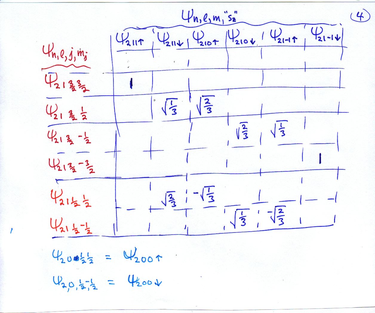
Those are hard questions. In a way, this is a preview of things that will be covered in Physics 139. One key consequence is that it changes the energies of the states a little bit, of order $10^{-4}$ eV. Equally or more important, it changes the fundamental structure and nature of the degeneracies. Instead of an eightfold degenerate 1st-excited state, one ends up with 6 and 2-fold degeneracies. The eigenstates are specific linear combinations of our "original" eigenstates.

If you get to the end of this and want to see more, maybe post a comment. That will give me some motivation to continue the story.


Here are two more pages. Please feel free to continue the discussion her or in the comments of the HW9 post.


Tuesday, February 26, 2013

Cool states.


I am experimenting with some new (to me) technologies and I thought i would share some of that here. Do these giffs show up okay in your browser? Can you guess what is being shown in each of these animations?

Monday, February 25, 2013

Wave packet propagation / special project.

This is a post on wave packet propagation, in free space and in a crystal lattice, and a suggestion for a special project if anyone has time for that.
Can you guess what this first giff shows?
(ps. this post contained a number of errors originally. i edited it, hopefully fixing them, on Feb 26.)


A lot of our discussion of electron movement in semiconductors is based on a belief in electron states that are somewhat localized (maybe within 20 lattice sites or therabouts), which maintain their integrity for some bit of time, and can move in a crystal. This belief is based in wave-packet theory. Here is an outline of how one might make some single-electron wave-packet states in free space or in a crystal:
Free space:
In free space we would use the spatial energy eigenstates, $e^{ikx}$ to make the wave packet. (One always has to use the energy eigenstates. In a crystal they are more complex.) In free space they are all of the form $e^{ikx}$ and have energies of $E(k) = \hbar^2 k^2/(2m)$.

A typical wave-packet state is a mixed state made of lots of these energy eigenstates, each with its appropriate time dependence. For example.

$\Psi(x,t) = \int g(k) e^{-ikx} e^{-i \omega(k) t} dk$

where
$g(k) = \sqrt{30/\pi} e^{-30^2 (k-\pi/20)^2}$.

The E vs k relationship:
$E(k) = \hbar^2 k^2/(2m)$,

leads to something like:
$\omega (k)  = 1972 (3 \times 10^{18}) k^2/(1.022 \times 10^6)$
where k is in inverse angstroms (and c in there is in angstroms/second.)

For  an electron in a crystal the E vs k relationship is different:
$\omega (k) =  (E_o - (B/2) cos (kb))/\hbar$
              $= (-10/6.6-(2/6.6) cos(k)) \times 10^{16}$
for a crystal with b = 1 Angstrom,  B/2 = 2 eV and with $\hbar$ in eV-sec.
(With k in inverse angstroms.)
(Hmmm. It might be better to program with hbar in eV-picoseconds and then have t in picoseconds in the equation for Psi. (Smaller exponents))

Also, the energy eigenstates would be different for an electron in a crystal. (They would be the Bloch states created by a sum over all the lattice sites that we talk about a lot.) I think that at low k, near the bottom of the conduction band, these long wave-length states are pretty similar to free electron states. A bit surprising, but i think it is true.

Anyway, I think what either of those two possibilities will give you is a one-electron wave-packet state that starts out about 10 or 20 lattice spacings (Angstroms) wide and moves to the right as a function of time. The reason I think it moves to the right is that the k values that are used center around k=pi/20, which is positive.  I think the packet profile, g(k), is pretty narrow in k; that was my intention.

One could start by just integrating (over k) at t=0 to investigate the nature of $\Psi (x,0)$. The integral is from k = -infinity to infinity.

And then try a small finite t and integrate (k) again to see the difference.

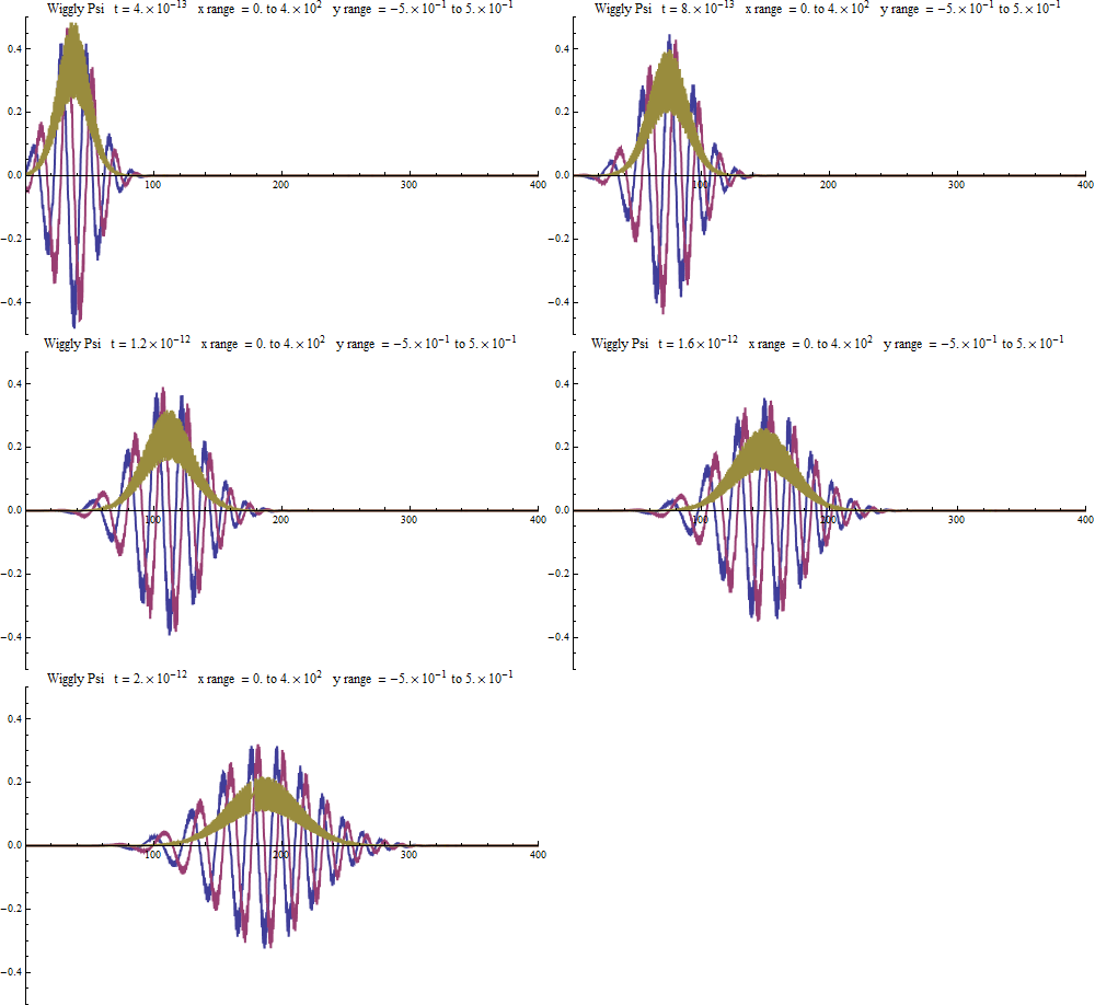
Here is an intriguing result from using a pretty narrow (in k) gaussian "packet" of crystal states centered at k=pi/10.


Midterm Scores

Below pleased find a sheet with midterm scores with names removed. I would like to tell you that anyone in the class can still get "an A". If you do much better on the final, that will be taken into account so that you can get a grade that reflects your actual understanding. This will not effect anyone else. There is not limit on the number of high grades that can be earned.

One of the main values of a midterm is to prepare you for the final, which will be similar in style and approach. Sometimes having a clear idea what to expect can be very helpful. There will not be any tricks. As in this midterm, I will basically tell you what will be on the test -- what will be asked. It may be useful to look back through the midterm preparation posts and see how they could have helped you more. I think they previewed every problem except 4b and 7 (and even those to some degree).

Since there are some inherent uncertainties in grading, I would like to give everyone a "+5". That is, you actually get a score 5 pts higher than what you see. That takes into account the possibility that you may have been graded too harshly or misunderstood. However, if you want to see about getting more points (regrading), you will be starting from your actual score and working up from there. Does that make sense? This is basically to avoid inadvertently having a system that penalizes people who do not dispute their score. Unless you find something really dramatic, it is often better to spend your
time studying and learning.
------------------

Sunday, February 24, 2013

PN Junction: initiating recombination and how that leads to light emission.

This video seeks to explain the essential physics of a light emitting diode. A light emitting diode is  a p-n junction in which an applied voltage creates a current flow that leads to electrons falling from the conduction band to the valance band, and in the process emitting light (photons). (Each electron that falls emits one photon.)

I think one can understand this physics without getting into the messy details of the "depletion region" at the interface of the p and n-type regions, or the difficult calculations that explain the unusual I-V characteristics of a pn junction. I am interested to get your feedback on how well this works. Do these explanations seem understandable, valid and interesting to you?


Friday, February 22, 2013

Homework 8:

suggested activities:  Watching the videos in the Feb 21 class notes post. Also, it may be helpful to read about moderately doped semiconductors and carrier generation and recombination processes in semiconductors. Also, p-n junctions, but just the most superficial things. I think we can understand them in a simple yet accurate manner. We will focus on p-n junction LEDs, lasers and solar cells.

8. $v= (Bbc/2\hbar c) sin(kb) = (Bbc/2\hbar c) (\pi/20)$
     = (4 eV 1 A/(2 1972 eV-A))  (pi/20) c
     = 4.8x10^6 cm/sec


9. One more problem! (the focus of this problem is to help you build your skills of actually calculating numbers.)
Consider an electron in the conduction band of a crystal for which the energy is given by:
$E_c (k) =  E_o - (B/2) cos (kb)$.
Then confirm that,
$v(k) = (Bb/2 \hbar) sin(bk)$,
and, for the case b = 1 angstrom and B=4 eV,
a) calculate v(k) at $k = \pi /(20 b)$ in Angstoms per second and in cm/sec. Get numbers!   (Soon we may try to show (numerically) that this is the electron speed associated with this state.)


Due Friday, 3 PM

1. a) If a semiconductor has a band gap of 1 eV what frequency of photon would you require in order to create an electron-hole-pair excitation? What color is that?

b) What color of photon would a semiconductor with a 1.9 eV band gap emit in a transition from the bottom of the conduction band to the top of the valence band?


2. Suppose you have a 1-dimensional semiconductor that is 2 cm long. Suppose the left half is doped with 10^4 acceptors per cm and the right half is doped with 10^4 donors per cm.

a) graph the density of electrons in the conduction band and the density of holes in the valence band (empty states) as a function of x. You can call the density of electrons in the conduction band, n, and the density of holes in the valence band, p.
(hint: don't make this too complicated. It is really simple!)


3. Consider a 1D semiconductor, our typical one, with a band gap of 0.5 eV between the top of the valence band and the bottom of the conduction band. Suppose you substitution dope the right-hand half of it with 10^4 donor atoms per cm and then apply a voltage (electron field) that pushes the mobile electrons in the conduction band (on the right) toward the left, into an region where they all fall into the valence band with each one emitting a photon. Let's assume that, in response to the applied voltage, the electrons move with a speed of 3 $10^6$ cm/sec.
a1) sketch a picture of that...

a2) Would the region on the left where the downward transition takes place need to be doped at all? why or why not? In what way would you dope it to allow downward "recombination" transitions. 

b) How many photons would be emitted per second?

c) what would be the energy of each photon (more or less)?

d) how much total power would be emitted? (in eV/sec, and Joules/sec = Watts)


4. Now consider a 3D semiconductor with a band gap of 0.5 eV and doped on the right-hand half of it with 10^17 donors/cm^3. Apply a voltage (electron field) that pushes those electrons toward the left (at a speed of 3 $10^6$ cm/sec) into a region on the left where they all fall into the valence band with each one emitting a photon.

a) would the region on the left need to be doped? In what way? Why?

b) How many photons would be emitted per second? (are the units the same or different than in #3? Why?)

c) what would be the energy of each photon (more or less)?

d) how much total power would be emitted? (what are the units of that?)

5. a) What semiconductor band gap would be best suited to creating a red LED?
b) a) What semiconductor band gap would be best suited to creating a green LED?

6. Discuss how substituting N in GaAs might possibly help you obtain a green LED (i.e., help you change a red LED material into a green one?)

7.  Consider a 1D semiconductor with an energy gap of 0.8 eV. Suppose the density of states near the bottom of the conduction band is g(E) = $2 \times 10^9$ states/(eV-cm). Further, suppose we treat g(E) as constant within the band and zero in the band gap).
a) sketch a plot of this approximate g(E) (which is either zero or $2 \times 10^9$ states/(eV-cm)).
b) Integrate the product g(E) times f(E) over the range of the conduction band,  where f(E) is the Fermi function. Put the Fermi energy $E_F$ right in the middle of the gap and set KT=0.025 eV = 1/40 eV.
(important hints:
 hint 1) What is the largest value of f(E) for E in the range of the conduction band? If it is small, then you can ignore the +1 in the denominator and the integrand becomes much easier. Perhaps if you are lucky the integrad becomes a constant, g(E), times a simple decaying exponential? (Do you feel lucky?)
  hint 2) The upper limit of integration (from the top of the conduction band) will give you a very, very, very small number. I would suggest that you totally ignore it.)
c) What are the units of your result from b)?
What is the numerical value of your result? (Do you need to have anything else given?)
d) Explain why this calculation might give you the density of electrons in the conduction band at room temperature for this semiconductor when it is un-doped (intrinsic).

8. a)  What is the relationship between the structure of diamond and the structure of Silicon?
b) Comparing the C-C bond in Diamond, and the C-C bond in Graphene: which is strongest? Why do you think that might be?

Appendix:
The Fermi function is:
$f(E) = (e^{(E-E_F)/KT} + 1)^{-1}$.
It tells you the probability, in a thermal physics/statistical physics sense, that a particular state at energy E is occupied. Note that it can't be bigger than 1 (Fermions) or less than zero.
You are given that KT= .025 eV (so you don't need to know K) and also where $E_F$ is (in the center of the gap).  Note that whenever $E-E_F$ is greater than about 3KT you can approximate f(E) by a simple exponential.

Student researcher position available.

I am looking for an undergraduate student to work next year as a research assistant on a project in which we calculate electron states in unusual materials. These will tend to be materials that have interesting quantum physics characteristics and possible potential for future device applications. Examples include topological insulators. The calculations are doing using a LINUX based program called FPLO (full potential, local orbitals), which you can check out online, so some expertise with LINUX type computing would be ideal. The program is all up and working, but it is not easy (for me) to run. (The undergrad setting it up now seems to do just fine, however.) I hope/expect to have funding to pay for about 160 hours or maybe more, i.e., about 20 weeks at 8 hours per week. This would likely involve a close collaboration with Arthur Ramirez, a physicist from Bell Labs who is now Dean of Engineering at UCSC, who is interested in these materials and does experiments on them. If interested, please email me at zacksc@gmail.com